
- English
- Español
- Português
- русский
- Français
- 日本語
- Deutsch
- tiếng Việt
- Italiano
- Nederlands
- ภาษาไทย
- Polski
- 한국어
- Svenska
- magyar
- Malay
- বাংলা ভাষার
- Dansk
- Suomi
- हिन्दी
- Pilipino
- Türkçe
- Gaeilge
- العربية
- Indonesia
- Norsk
- تمل
- český
- ελληνικά
- український
- Javanese
- فارسی
- தமிழ்
- తెలుగు
- नेपाली
- Burmese
- български
- ລາວ
- Latine
- Қазақша
- Euskal
- Azərbaycan
- Slovenský jazyk
- Македонски
- Lietuvos
- Eesti Keel
- Română
- Slovenski
- मराठी
- Srpski језик
Қытай CVD SIC Өндірушілер, Жабдықтаушылар, Зауыт
CVD SiC is a vacuum deposition process used to produce high-purity solid materials. This process is often used in semiconductor manufacturing to form thin films on wafer surfaces. During the chemical vapor deposition (CVD) process for producing silicon carbide (SiC), a substrate is exposed to one or more volatile precursors, which chemically react on the substrate surface to form the desired SiC deposit. Among the various methods for producing SiC, CVD produces products with high uniformity and purity, and offers strong process controllability.
Simply put, CVD SiC refers to SiC produced via the chemical vapor deposition (CVD) process. In this process, gaseous precursors, typically containing silicon and carbon, react in a high-temperature reactor to deposit a thin SiC film onto a substrate. CVD SiC is valued for its exceptional properties, including high thermal conductivity, chemical inertness, mechanical strength, and resistance to thermal shock and wear. These properties make chemical vapor deposited (CVD) silicon carbide (SiC) ideal for demanding applications such as semiconductor manufacturing, aerospace components, armor, and high-performance coatings. This material's exceptional durability and stability under extreme conditions ensure its effectiveness in improving the performance and lifespan of advanced technologies and industrial systems.
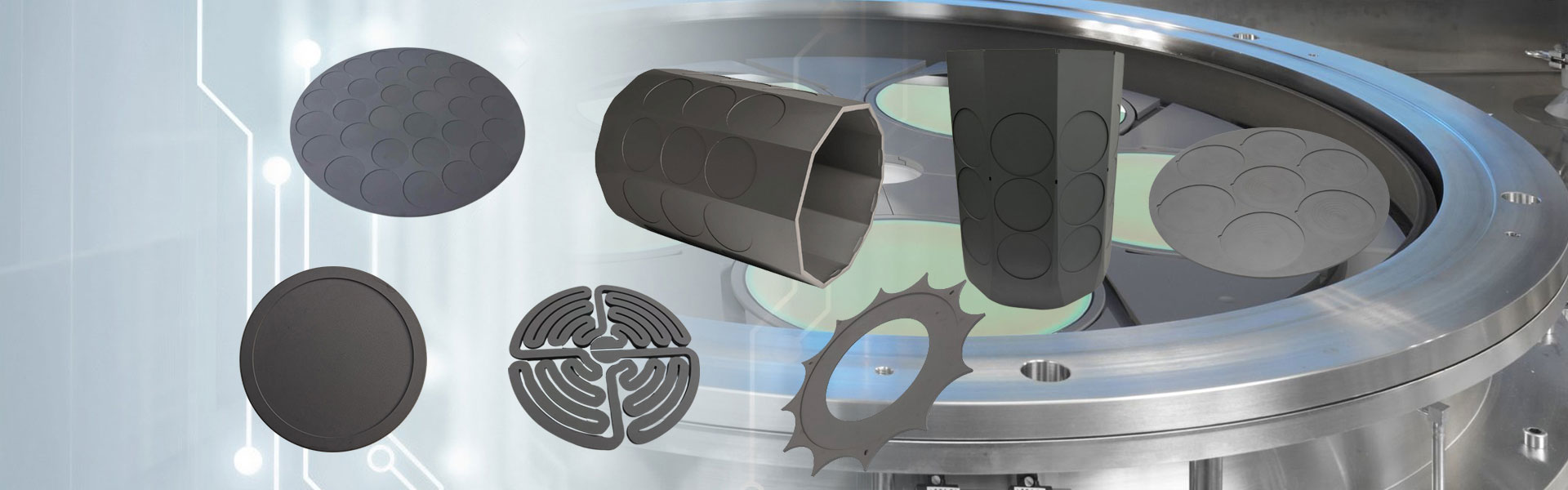
CVD SiC materials, due to their unique combination of excellent thermal, electrical, and chemical properties, are well-suited for applications in the semiconductor industry, where high-performance materials are required. Chemical vapor deposited (CVD) silicon carbide (SiC) components are widely used in etching equipment, MOCVD equipment, Si and SiC epitaxy equipment, and rapid thermal processing equipment.
The largest market segment for CVD SiC components is etching equipment components. Due to its low reactivity to chlorine- and fluorine-containing etching gases and its electrical conductivity, CVD silicon carbide (SiC) is an ideal material for components such as focus rings in plasma etching equipment. CVD silicon carbide (SiC) components in etching equipment include focus rings, gas showerheads, trays, edge rings.
Take the focus ring, for example. This critical component is placed outside the wafer and in direct contact with it. Voltage is applied to the ring to focus the plasma passing through it, thereby focusing the plasma on the wafer and improving processing uniformity. Traditionally, focus rings are made of silicon or quartz. However, with the advancement of integrated circuit miniaturization, the demand for and importance of etching processes in integrated circuit manufacturing continues to increase. The power and energy of the plasma used for etching are also increasing, especially in capacitively coupled plasma (CCP) etching equipment, which requires even higher plasma energies. Consequently, focus rings made of silicon carbide are becoming increasingly popular.
Due to the high performance of CVD SiC and its ability to be sliced into very thin sections, it can also benefit sputter targets and all types of electrodes.
Process of Chemical Vapor Deposition (CVD)
CVD is a process that transforms a material from a gas phase to a solid phase, used to form a thin film or coating on a substrate surface. The following are the basic steps in CVD:
1. Substrate Preparation
Choose an appropriate substrate material and perform the appropriate cleaning and surface treating to produce a clean, flat surface with good adhesion.
2. Reactive Gas Preparation
Prepare the necessary amount of reactive gas or vapor and inject it into the deposition chamber by some means (gas supply system). The reactive gas can be an organic compound, a metal-organic precursor, inert gas, or other gaseous species.
3. Deposition Reaction
If all instrumentation is setup correctly the CVD process will begin under the pre-defined reaction conditions. The reactive gas that has been injected into the chamber will undergo some chemical or physical reaction on the substrate surface to form a deposit onto the substrate surface. The deposit formation can be the result of several types of processes depending on the deposition method, these include vapor-phase thermal decomposition, chemical reaction, sputtering, epitaxial growth, etc.
4. Control and Monitoring
At the same time during the deposition process, certain deposition parameters need to be controlled and monitored in real time if the observer wishes to ensure the best possible properties in the film are maintained. These include relevant temperature measurement, pressure monitoring, and regulation of gas flow, all the while aiming to keep the desired reaction conditions stable and constant.
5. Deposition Completion and Post-Processing
When either the deposition time, predetermined thickness, or method selected, is achieved the introduction of the reaction gas can be ceased and deposition process ended. Following the deposition, several pertinent post-processing methods (annealing, structural modifications, surface treatment, etc.) should be performed to improve the film performance/quality.
It's important to note that the specific vapor deposition process can vary depending on the deposition technology, material type, and application requirements. However, the basic process outlined above covers most common vapor deposition steps.


- View as

Жоғарғы электродты жерге қосу сақинасы
Semicorex Upper Electrode Grounding Ring - электрлік потенциалды тұрақтандыратын және жартылай өткізгіштерді өңдеу және тұндыру жүйелерінде біркелкі плазманың таралуын қолдайтын ультра жоғары таза CVD SiC плазмалық басқару компоненті. Semicorex дәл CVD SiC жерге қосу сақиналары мен плазмалық жартылай өткізгіш компоненттерін бүкіл әлем бойынша жеткізеді, жартылай өткізгіш жабдықтардың жетекші өндірушілеріне теңшелген өлшемдерді, электрлік қасиеттерді және сенімді жаһандық жеткізуді ұсынады.*
Ары қарай оқуСұрау жіберу
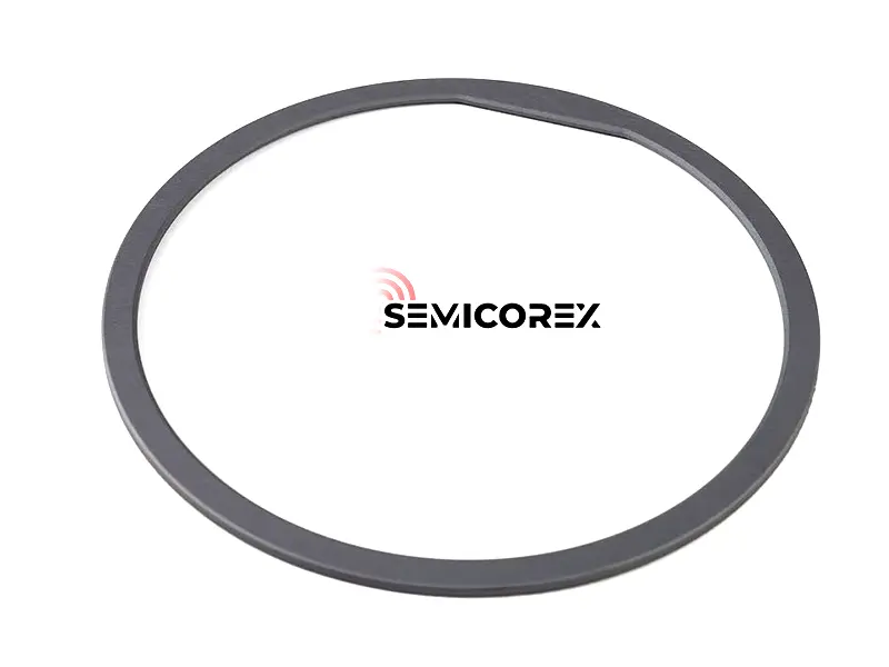
Оюдың жиегі сақинасы
Semicorex Etch Edge Ring – пластинаның жиегі айналасындағы плазманың таралуын бақылайтын, тегістеу біркелкілігін, процестің дәлдігін және жартылай өткізгіштерді өндірудің жалпы өнімділігін жақсартатын жоғары таза CVD SiC плазмамен қапталған компонент. Semicorex әлемдік жартылай өткізгіш өндірушілерге CVD SiC фокустауыш сақиналарын, жерге қосу сақиналарын, душ бастиектерін және теңшелген плазмалық бақылау құрамдастарын ұсынады.
Ары қарай оқуСұрау жіберу
CVD SiC Fin
Semicorex CVD SiC Fin - бұл Chemical Vapor Deposition компаниясы шығарған қалың, жоғары тығыздықтағы қатты кремний карбид компоненті, ерекше тазалықты, беріктікті және коррозияға төзімділікті қажет ететін плазмамен қапталған және өте жоғары температуралы жартылай өткізгіш қолданбаларға арналған. Semicorex бүкіл әлем бойынша жартылай өткізгіш жабдық өндірушілеріне CVD кремний карбидінің жетілдірілген компоненттерін жеткізеді, бұл реттелетін шешімдерді, дәл инженерияны және ең талап етілетін технологиялық орталар үшін сенімді жаһандық жеткізуді қамтамасыз етеді.*
Ары қарай оқуСұрау жіберу
Жартылай өткізгіштерге арналған керамикалық фокус сақиналары
Жартылай өткізгіштерге арналған Semicorex керамикалық фокус сақиналары - бұл жоғары қарқынды плазмалық өңдеу орталары үшін арнайы әзірленген CVD SiC материалдарынан жасалған жоғары өнімді сақина бөліктері. Semicorex - жартылай өткізгіштерге арналған CVD SiC керамикалық фокус сақиналарының жетекші өндірушісі, біз сіздің сұрауыңызды күтеміз.
Ары қарай оқуСұрау жіберу
2L10-506419-21 үшін CVD SiC фокус сақинасы
Жоғары өнімді CVD SiC материалдарынан жасалған, 2L10-506419-21 үшін Semicorex CVD SiC фокус сақинасы дәл жартылай өткізгіштерді өңдеу процестерінде қолданылатын TEL VIGUS RK4 жабдығы үшін арнайы өңделген шешуші сақина бөлігі болып табылады. Semicorex таңдау дәл және біркелкі өңдеу нәтижелеріне қол жеткізу үшін CVD SiC тамаша шешімдерін алатыныңызды білдіреді.
Ары қарай оқуСұрау жіберу
Қатты кремний карбидті қанаттар
Semicorex қатты кремний карбидті қанаттары - бұл негізінен жартылай өткізгішті термиялық өңдеу жабдығындағы жоғары температуралы пештерде қолданылатын қатты CVD SiC-тен өңделген дәлдіктегі жоғары өнімді құрамдас бөліктер. Semicorex компаниясы біздің қымбат тұтынушыларымыз үшін нарықтағы жетекші сапаға ие тапсырыс бойынша жасалған қатты кремний карбидті қалқандарды ұсынуға ұмтылады және сіздің Қытайдағы ұзақ мерзімді серіктестеріңіз болуды асыға күтеді.
Ары қарай оқуСұрау жіберу
Semicorex көптеген жылдар бойы CVD SIC шығарады және Қытайдағы кәсіби CVD SIC өндірушілер мен жеткізушілердің бірі болып табылады. Жаппай қаптаманы қамтамасыз ететін біздің жетілдірілген және ұзақ мерзімді өнімдерімізді сатып алғаннан кейін, біз жылдам жеткізудің үлкен мөлшеріне кепілдік береміз. Жылдар бойы біз тұтынушыларға теңшелген қызмет көрсеттік. Клиенттер біздің өнімдерімізге және тамаша қызметімізге қанағаттанады. Біз сіздің сенімді ұзақ мерзімді іскер серіктес болуды шын жүректен күтеміз! Біздің зауыттан өнімдерді сатып алуға қош келдіңіз.